Tidak ada produk di dalam troli.
Kembali Ke TokoSitus web ini menggunakan cookie untuk meningkatkan pengalaman Anda. Kami akan menganggap Anda setuju dengan hal ini, tetapi Anda dapat menolaknya jika Anda mau. Baca Lebih Lanjut
#### **I. Core Market Landscape in 2025**
1. **Market Size & Growth**
– **Global Scale**: The global PCB market is projected to reach **$96.8 billion** in 2025, with a CAGR of **5.8%**, driven by 5G, automotive electronics, and IoT demand .
– **China’s Dominance**: China leads global PCB production, accounting for 43.7% of high-layer PCBs ($1.058 billion) and significantly increasing its share in HDI boards .
2. **Industry Transformation**
– **Value over Volume**: The sector is shifting from capacity expansion to high-value product R&D (e.g., high-layer PCBs, HDI, IC substrates), with smart manufacturing penetrating the entire chain .
– **Equipment Market Surge**: Global PCB equipment sales will hit **$7.79 billion**, fueled by China’s policy-backed localization push .
3. **Challenges & Opportunities**
– Key hurdles include geopolitical supply-chain risks, rising material costs, and reliance on imported high-end equipment .
– Green manufacturing (low-carbon processes) and industry collaboration (equipment-material-design synergy) are critical growth levers .
🌐 **II. 2026 Global Trends Forecast**
1. **Demand Surge: AI Computing Drives Structural Growth**
– **AI-Specific PCBs**: The global AI PCB market is set to soar to **$10 billion (¥69.3 billion)** in 2026, up **64% YoY** .
– **Key Growth Segments**:
– **AI Server PCBs**: Market to exceed **$16 billion**, with per-rack value **3–10× higher** than traditional servers (due to complex wiring/thermal demands) .
– **ASIC-Chip PCBs**: Emerging as a major demand driver for custom computing chips .
2. **Technology Shifts**
– **Advanced Layering & Packaging**: 18+-layer PCBs and substrate technologies will rise to meet AI/HPC needs .
– **Smart Manufacturing Adoption**: AI-powered inspection and automation will boost yield and output .
3. **Supply-Demand Dynamics**
– **Persistent Shortages**: AI PCBs face tight supply due to high technical barriers and slow capacity ramp-up .
– **Competitive Landscape**: Chinese firms gain ground in HDI/high-layer PCBs but lag in advanced IC substrates .
📊 **III. Key Data Comparison (2025 vs. 2026)**
| **Segment** | **2025** | **2026 Projection** |
|————————-|——————————-|—————————–|
| Global PCB Market |$96.8B | >$100B (5.8% CAGR) |
| AI PCB Market | ~$6B (est.) | **$10B** (+64%) |
| Equipment Market |$7.79B | >$8.5B (smart manufacturing)|
| China’s High-Layer PCB Share | 43.7% | >50% |
#### ⚠️ **IV. Strategic Implications**
1. **Risks**:
– Geopolitical supply-chain fragmentation (e.g., equipment import restrictions) .
– Potential shortages of high-frequency materials/copper foil .
2. **Recommendations**:
– **Tech Leadership**: Prioritize R&D for AI server/advanced packaging PCBs (20+ layers).
– **Agile Capacity**: Invest in smart production lines for demand flexibility.
– **Sustainability**: Comply with carbon regulations (e.g., EU CBAM) .
💎 Conclusion
The PCB industry reaches an **inflection point in 2025**, transitioning toward value-driven growth. **2026 will witness an AI-driven demand explosion**, with high-barrier segments (multilayer PCBs, IC substrates) becoming competitive battlegrounds. Chinese manufacturers must accelerate breakthroughs in equipment/material independence to capitalize on global supply-chain restructuring .
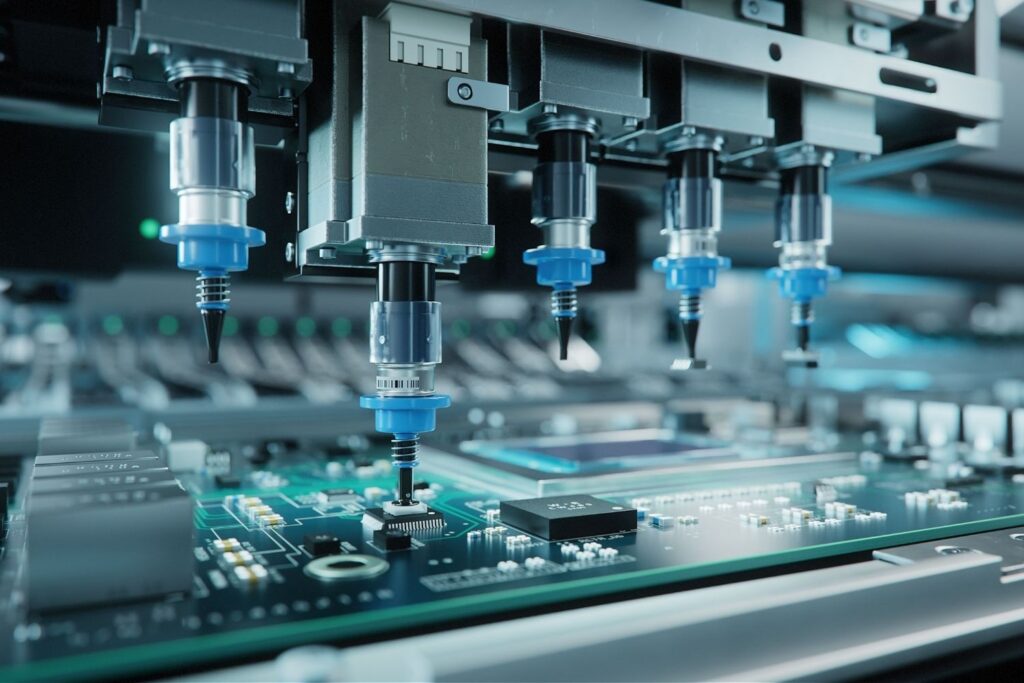
Peralatan Manufaktur SMT:
Pilih dan Tempatkan Mesin
Penembak Chip
Mesin Penempatan Kecepatan Tinggi
Mesin Penempatan Ultra Presisi
Oven Aliran Ulang
Mesin Solder Gelombang
Mesin Solder Selektif
Printer Tempel Solder
Mesin Inspeksi Optik Otomatis (AOI)
Sistem Inspeksi XRay (XRAY)
Sistem SPI 3D (Inspeksi Pasta Solder)
Sistem Uji Kelistrikan Otomatis (ATE)
Penguji Probe Terbang
Dalam Penguji Sirkuit (ICT)
Pembersih Ultrasonik
Sistem Pembersihan Berair
Sistem Pembersih Pelarut
Generator Nitrogen untuk Kontrol Oksidasi
Sistem Konveyor
Sistem Pengumpan (untuk komponen)
Pemuat / Pembongkar PCB
Penghitung Komponen
Perangkat Lunak Pemrograman Mesin Penempatan
Perangkat Lunak CAD/CAM untuk Desain dan Manufaktur
Perangkat Lunak Pengumpulan dan Analisis Data
Peralatan Celup:
Mesin Solder Gelombang Tunggal
Mesin Solder Gelombang Ganda
Mesin Solder Gelombang Bebas Timbal
Sistem Solder Selektif Robotik
Unit Penyolderan Selektif Atas Bangku
Stasiun Solder Celup Manual
Mesin Solder Gelombang Semi Otomatis
Peralatan Solder Pelat Panas
Dispenser Fluks
Aplikator Busa Fluks
Sistem Semprotan Fluks
Klem Tepi PCB
Sistem Pengindeksan Papan
Sabuk Konveyor untuk Transportasi Papan
Sistem Pembersihan Ultrasonik untuk Papan Melalui Lubang
Sistem Pembersihan Sikat
Sistem Pembersihan Uap IPA
Alat Inspeksi Visual
Multi meter dan Penguji Kontinuitas
Osiloskop untuk Pengujian Integritas Sinyal
Penguji Fungsional untuk Rakitan yang Telah Selesai
Pot dan Batang Solder
Suku Cadang untuk Mesin Solder Gelombang
Nozel dan Tip untuk Pot Solder
Alat Pematrian dan Kepang
Daftar ini mencakup peralatan utama yang biasanya ditemukan di www.v2smt.com, yang melayani proses penyolderan SMT dan melalui lubang (celup). Setiap item dalam panduan komprehensif ini sangat penting dalam menjamin perakitan elektronik yang berkualitas tinggi, efisien, dan dapat diandalkan.
V2SMT Hak Cipta © 2026 Semua Hak Dilindungi Undang-Undang.
Situs web ini menggunakan cookie untuk meningkatkan pengalaman Anda. Kami akan menganggap Anda setuju dengan hal ini, tetapi Anda dapat menolaknya jika Anda mau. Baca Lebih Lanjut
| Nama | Domain | Tujuan | Kadaluarsa | Jenis |
|---|---|---|---|---|
| wpl_user_preference | v2smt.com | Preferensi Persetujuan Cookie WP GDPR. | 1 tahun | HTTP |
| Nama | Domain | Tujuan | Kadaluarsa | Jenis |
|---|---|---|---|---|
| sbjs_migrasi | v2smt.com | Cookie pelacakan Sourcebuster | 55 tahun | HTTP |
| sbjs_current_add | v2smt.com | Cookie pelacakan Sourcebuster | 55 tahun | HTTP |
| sbjs_first_add | v2smt.com | Cookie pelacakan Sourcebuster | 55 tahun | HTTP |
| sbjs_current | v2smt.com | Cookie pelacakan Sourcebuster | 55 tahun | HTTP |
| sbjs_first | v2smt.com | Cookie pelacakan Sourcebuster | 55 tahun | HTTP |
| sbjs_udata | v2smt.com | Cookie pelacakan Sourcebuster | 55 tahun | HTTP |
| sbjs_session | v2smt.com | Sesi Pelacakan SourceBuster | Sesi | HTTP |