No products in the cart.
Return To ShopThis website uses cookies to improve your experience. We'll assume you're ok with this, but you can opt-out if you wish. Read More
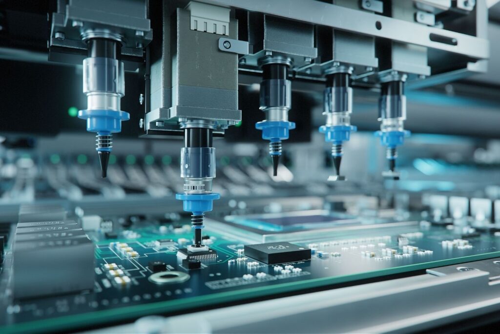
Understanding the “Invisible Killer” – The Deadly Impact of Ionic Contamination on PCBs
During manufacturing and assembly, printed circuit boards (PCBs) inevitably come into contact with contaminants like solder paste residues, human sweat, dust particles, and environmental pollutants. These substances contain conductive anions (e.g., Cl⁻, Br⁻) and cations (e.g., Na⁺, K⁺). Under power operation or humid conditions, they form electrolytic solutions that trigger dendritic growth and drastically reduce surface insulation resistance. This vicious cycle leads to short circuits, signal interference, and system malfunctions—silent threats compromising reliability.
Traditional visual inspection fails to detect such microscopic ionic residues. Only quantitative **ion contamination testing** provides objective cleanliness assessment—enter the domain where specialized testers shine. Our ICT series employs the industry-standard *ROSE method* (Solvent Extraction Technique), precisely calculating total ionic contamination by measuring conductivity changes in solvent extracts from cleaned samples.
Core Advantages of Our Ion Contamination Testers
✅ Ultra-High Precision
Meets stringent standards across demanding industries including aerospace and automotive electronics (compliant with IPC-J-STD-001 & IPC-TM-650 2.3.25). Delivers exceptional detection sensitivity for mission-critical applications.
✅ User-Friendly Efficiency
Intuitive touchscreen interface enables rapid mastery even for novice operators. One-click automated testing workflows generate instant reports while minimizing human error—dramatically improving QC throughput without expertise bottlenecks.
✅ Industrial-Grade Durability
Engineered for harsh production floor environments common in SME facilities. Corrosion-resistant components ensure long-term stability under intensive daily use, slashing maintenance costs over lifecycle deployment.
✅ Universal Compatibility
Validates cleanliness across all PCB material types (high-frequency laminates, flexible substrates) and surface finishes—from bare boards to fully assembled units (PCBAs). Supports full supply chain quality control.
Transform raw measurement values into actionable process insights through closed-loop optimization:
Incoming QC Auditing
Screen raw materials like copper-clad laminates and prepreg sheets at intake stages to block contaminated batches before downstream processing begins.
▪️ Critical Process Monitoring
Verify etching solution removal after pattern plating; validate resist stripping efficacy post imaging; assess pre/post-curing cleanliness of solder mask layers; monitor bath fluid purity in immersion gold/tin systems.
▪️ Post-Reflow Verification
Regular sampling of assembled boards post soldering confirms cleaner effectiveness, optimizes flux application parameters, establishes enterprise-specific cleanliness benchmarks, and enables tiered acceptance criteria based on product grade (consumer/industrial/automotive).
▪️ Failure Analysis
When field failures occur, pinpoint ionic contamination as root cause through targeted testing—providing definitive evidence for troubleshooting teams.
| Sector | Use Case Examples |
| Electronics Mfg | • PCB etch verification<br>• Solder paste residue detection<br>• BGA/CSP cleaning validation |
| R&D Labs | • Material purity studies<br>• Cleaning process qualification<br>• Environmental stress screening |
| Automotive Elec | • ECU controller boards<br>• ADAS sensor modules<br>• Battery management systems (BMS) |
| Telecommunications| • 5G base station transceivers<br>• Optical amplifier modules<br>• High-speed backplane testing |
| Aerospace/Defense | • Flight control avionics<br>• Missile guidance systems<br>• Satellite communication arrays |
| Medical Devices | • Pacemaker mainboards<br>• Neural stimulator controls<br>• Patient monitor electronics |
| Specialized Equipment | • Marine navigation systems<br>• Offshore monitoring gear<br>• Wind turbine controllers<br>• Substation communication nodes |
This powerful diagnostic tool transforms invisible risks into manageable metrics, enabling manufacturers to achieve unprecedented process control from raw material receipt through final assembly. By converting contamination data into corrective actions, companies realize significant yield improvements while building zero-defect cultures across global supply chains.
Pick and Place Machines
Chip Shooters
High Speed Placement Machines
Ultra Precision Placement Machines
Reflow Ovens
Wave Soldering Machines
Selective Soldering Machines
Solder Paste Printers
Automated Optical Inspection (AOI) Machines
XRay Inspection Systems (XRAY)
3D SPI (Solder Paste Inspection) Systems
Automated Electrical Test Systems (ATE)
Flying Probe Testers
In Circuit Testers (ICT)
Ultrasonic Cleaners
Aqueous Cleaning Systems
Solvent Cleaning Systems
Nitrogen Generators for Oxidation Control
Conveyor Systems
Feeder Systems (for components)
PCB Loaders/Unloaders
Component Counters
Placement Machine Programming Software
CAD/CAM Software for Design and Manufacturing
Data Collection and Analysis Software
Single Wave Soldering Machines
Double Wave Soldering Machines
LeadFree Wave Soldering Machines
Robotic Selective Soldering Systems
Bench top Selective Soldering Units
Manual Dip Soldering Stations
Semi Automatic Wave Soldering Machines
Hot Plate Soldering Equipment
Flux Dispensers
Flux Foam Applicators
Flux Spray Systems
PCB Edge Clamps
Board Indexing Systems
Conveyor Belts for Board Transport
Ultrasonic Cleaning Systems for Through Hole Boards
Brush Cleaning Systems
IPA Vapor Cleaning Systems
Visual Inspection Tools
Multimeters and Continuity Testers
Oscilloscopes for Signal Integrity Testing
Functional Testers for Completed Assemblies
Solder Pots and Bars
Spare Parts for Wave Soldering Machines
Nozzles and Tips for Solder Pots
Desoldering Tools and Braids
This list encompasses the primary equipment typically found at www.v2smt.com, which caters to both SMT and through hole (dip) soldering processes. Each item in this comprehensive guide is pivotal in guaranteeing high quality, efficient, and dependable electronic assembly.
V2SMT Copyright © 2026 All Rights Reserved.
This website uses cookies to improve your experience. We'll assume you're ok with this, but you can opt-out if you wish. Read More
| Name | Domain | Purpose | Expiry | Type |
|---|---|---|---|---|
| wpl_user_preference | v2smt.com | WP GDPR Cookie Consent Preferences. | 1 year | HTTP |
| Name | Domain | Purpose | Expiry | Type |
|---|---|---|---|---|
| sbjs_migrations | v2smt.com | Sourcebuster tracking cookie | 55 years | HTTP |
| sbjs_current_add | v2smt.com | Sourcebuster tracking cookie | 55 years | HTTP |
| sbjs_first_add | v2smt.com | Sourcebuster tracking cookie | 55 years | HTTP |
| sbjs_current | v2smt.com | Sourcebuster tracking cookie | 55 years | HTTP |
| sbjs_first | v2smt.com | Sourcebuster tracking cookie | 55 years | HTTP |
| sbjs_udata | v2smt.com | Sourcebuster tracking cookie | 55 years | HTTP |
| sbjs_session | v2smt.com | SourceBuster Tracking session | Session | HTTP |