カートに商品がありません。
ショップに戻るこのウェブサイトでは、お客様の利便性を向上させるためにクッキーを使用しています。ご希望であればオプトアウトすることも可能です。 続きを読む
#### **I. Core Market Landscape in 2025**
1. **Market Size & Growth**
– **Global Scale**: The global PCB market is projected to reach **$96.8 billion** in 2025, with a CAGR of **5.8%**, driven by 5G, automotive electronics, and IoT demand .
– **China’s Dominance**: China leads global PCB production, accounting for 43.7% of high-layer PCBs ($1.058 billion) and significantly increasing its share in HDI boards .
2. **Industry Transformation**
– **Value over Volume**: The sector is shifting from capacity expansion to high-value product R&D (e.g., high-layer PCBs, HDI, IC substrates), with smart manufacturing penetrating the entire chain .
– **Equipment Market Surge**: Global PCB equipment sales will hit **$7.79 billion**, fueled by China’s policy-backed localization push .
3. **Challenges & Opportunities**
– Key hurdles include geopolitical supply-chain risks, rising material costs, and reliance on imported high-end equipment .
– Green manufacturing (low-carbon processes) and industry collaboration (equipment-material-design synergy) are critical growth levers .
🌐 **II. 2026 Global Trends Forecast**
1. **Demand Surge: AI Computing Drives Structural Growth**
– **AI-Specific PCBs**: The global AI PCB market is set to soar to **$10 billion (¥69.3 billion)** in 2026, up **64% YoY** .
– **Key Growth Segments**:
– **AI Server PCBs**: Market to exceed **$16 billion**, with per-rack value **3–10× higher** than traditional servers (due to complex wiring/thermal demands) .
– **ASIC-Chip PCBs**: Emerging as a major demand driver for custom computing chips .
2. **Technology Shifts**
– **Advanced Layering & Packaging**: 18+-layer PCBs and substrate technologies will rise to meet AI/HPC needs .
– **Smart Manufacturing Adoption**: AI-powered inspection and automation will boost yield and output .
3. **Supply-Demand Dynamics**
– **Persistent Shortages**: AI PCBs face tight supply due to high technical barriers and slow capacity ramp-up .
– **Competitive Landscape**: Chinese firms gain ground in HDI/high-layer PCBs but lag in advanced IC substrates .
📊 **III. Key Data Comparison (2025 vs. 2026)**
| **Segment** | **2025** | **2026 Projection** |
|————————-|——————————-|—————————–|
| Global PCB Market |$96.8B | >$100B (5.8% CAGR) |
| AI PCB Market | ~$6B (est.) | **$10B** (+64%) |
| Equipment Market |$7.79B | >$8.5B (smart manufacturing)|
| China’s High-Layer PCB Share | 43.7% | >50% |
#### ⚠️ **IV. Strategic Implications**
1. **Risks**:
– Geopolitical supply-chain fragmentation (e.g., equipment import restrictions) .
– Potential shortages of high-frequency materials/copper foil .
2. **Recommendations**:
– **Tech Leadership**: Prioritize R&D for AI server/advanced packaging PCBs (20+ layers).
– **Agile Capacity**: Invest in smart production lines for demand flexibility.
– **Sustainability**: Comply with carbon regulations (e.g., EU CBAM) .
💎 Conclusion
The PCB industry reaches an **inflection point in 2025**, transitioning toward value-driven growth. **2026 will witness an AI-driven demand explosion**, with high-barrier segments (multilayer PCBs, IC substrates) becoming competitive battlegrounds. Chinese manufacturers must accelerate breakthroughs in equipment/material independence to capitalize on global supply-chain restructuring .
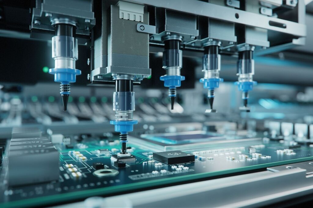
SMT製造装置:
ピック&プレースマシン
チップシューター
高速プレースメントマシン
超精密配置機
リフロー炉
ウェーブはんだ付け機
選択はんだ付け装置
ソルダーペーストプリンター
自動光学検査(AOI)装置
X線検査装置 (XRAY)
3D SPI(はんだペースト検査)システム
自動電気テストシステム(ATE)
フライングプローブテスター
インサーキットテスター(ICT)
超音波クリーナー
水系洗浄システム
溶剤洗浄システム
酸化抑制用窒素発生装置
コンベアシステム
フィーダーシステム(コンポーネント用)
PCBローダー/アンローダー
コンポーネント・カウンター
プレースメント・マシン・プログラミング・ソフトウェア
設計・製造用CAD/CAMソフトウェア
データ収集・分析ソフトウェア
ディップ装置:
単一波はんだ付け装置
ダブルウェーブはんだ付け装置
鉛フリーはんだ付け装置
ロボット選択はんだ付けシステム
卓上型選択はんだ付け装置
手動ディップはんだ付けステーション
半自動ウェーブはんだ付け装置
ホットプレートはんだ付け装置
フラックスディスペンサー
フラックスフォームアプリケーター
フラックス・スプレー・システム
PCBエッジクランプ
ボード・インデックス・システム
基板搬送用コンベアベルト
スルーホール基板用超音波洗浄システム
ブラシ洗浄システム
IPA蒸気洗浄システム
目視検査ツール
マルチメーターと導通テスター
シグナル・インテグリティ試験用オシロスコープ
完成品の機能試験機
はんだポットとバー
ウェーブソルダリングマシン用スペアパーツ
はんだポット用ノズルとチップ
はんだ除去ツールとブレイド
このリストには、一般的に以下のような主要機器が含まれている。 www.v2smt.com, は、SMTとスルーホール(ディップ)はんだ付けプロセスの両方に対応しています。この包括的なガイドの各項目は、高品質、効率的、信頼性の高い電子アセンブリを保証する上で極めて重要です。.
V2SMT Copyright © 2026 All Rights Reserved.
| 名称 | ドメイン | 目的 | 期限切れ | タイプ |
|---|---|---|---|---|
| wpl_user_preference | v2smt.com | WP GDPRクッキーの同意設定。 | 1年 | HTTP |
| 名称 | ドメイン | 目的 | 期限切れ | タイプ |
|---|---|---|---|---|
| sbjs_migrations | v2smt.com | ソースバスター・トラッキング・クッキー | 55年 | HTTP |
| sbjs_current_add | v2smt.com | ソースバスター・トラッキング・クッキー | 55年 | HTTP |
| sbjs_first_add | v2smt.com | ソースバスター・トラッキング・クッキー | 55年 | HTTP |
| sbjs_current | v2smt.com | ソースバスター・トラッキング・クッキー | 55年 | HTTP |
| sbjs_first | v2smt.com | ソースバスター・トラッキング・クッキー | 55年 | HTTP |
| sbjs_udata | v2smt.com | ソースバスター・トラッキング・クッキー | 55年 | HTTP |
| sbjs_session | v2smt.com | ソースバスター追跡セッション | セッション | HTTP |